• NUS Information Technology | NUS IT Services, Solutions & Governance
  • NUS Information Technology | NUS IT Services, Solutions & Governance
  • Get Quote
  • NUS Information Technology | NUS IT Services, Solutions & Governance
    NUS Information Technology | NUS IT Services, Solutions & Governance
    • Milestones
    • Getting Started
      • HPC Portal
      • Register for HPC
      • Registration Guide
      • Introductory Guide for New HPC Users
      • How to Run Batch Job
    • Services
      • Data Processing, Storage & Management
      • Application Software
      • HPC Consulting Service
      • HPC GPU
      • Parallel Computing
      • Scientific Visualisation
  • myEmail    Staff Portal    Student Portal    A.S.K.
Home Services HPC Newsletter » Interfacial Interaction between Metals and Monolayer MoS2 Revealed by First-Principles Calculations

INTERFACIAL INTERACTION BETWEEN METALS AND MONOLAYER MoS2 REVEALED BY FIRST-PRINCIPLES CALCULATIONS

By Dr. Yang Ming and Prof. Feng Yuan Ping, Institute of Materials Research and Engineering, A*STAR and Department of Physics, NUS on 27 Jun, 2017

The electrical contact between metals and semiconductors plays an increasingly important role in determining the electronic device performance when the device size is approaching nanoscale. Transition metal dichalcogenide monolayers (TMD) is a promising alternative to Si as channel material. However, it is challenging to obtain a low contact resistance for electrical contacts between metals and two-dimensional (2D) TMD materials. Even for low work function metals, with a work function comparable to the electron affinity of TMD monolayers, a sizable contact barrier height still occurs, which is due to the Fermi level pinning effect induced by the interaction between the metal and the TMD monolayer.

In this study, density-functional theory (DFT) based first-principles calculations were carried out to study the interfacial interaction between metals and monolayer MoS2, in which the Vienna ab initio simulation package (VASP5.4.1) was used with the projector augmented wave (PAW) pseudopotentials, the Perdew-Burke-Ernzerhof (PBE) exchange-correlation functionals, and plane-wave basis.

Our calculations show that for high work-function metal (Ni) on the monolayer MoS2, the interfacial interaction is strong, as supported by large adsorption energy, the formation of interfacial bonds, and significant charge redistribution on the MoS2 basal plane in Fig. 1.
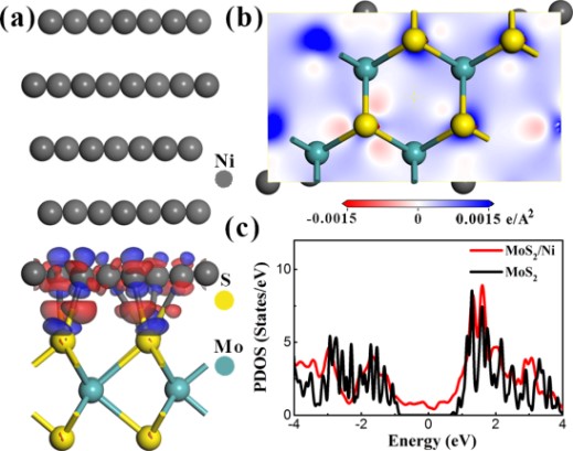
2 monolayer, in which the charge density difference is superimposed. (b) The contour plot of the charge density difference projected on the S plane near the Ni atoms. (c) The projected density of states (PDOS) of MoS2 monolayer in free standing form (black line) or in MoS2/Ni (111) case (red line), in which the Fermi energy is aligned to vacuum level.” width=”519″ height=”409″ /> Figure 1: (a) Side view of the most stable configuration for Ni (111) on MoS2 monolayer, in which the charge density difference is superimposed. (b) The contour plot of the charge density difference projected on the S plane near the Ni atoms. (c) The projected density of states (PDOS) of MoS2 monolayer in free standing form (black line) or in MoS2/Ni (111) case (red line), in which the Fermi energy is aligned to vacuum level.

When in contact with chemically more reactive Ni, the Mo-S bonds are weakened because of the formation of interfacial Ni-S bonds. The low lying unoccupied electronic states derived from Mo d orbitals spread into the band gap, forming the metallic states. These mid-gap states pin the Fermi level partially, resulting in a large Schottky contact barriers (0.72 eV) between Ni and monolayer MoS2.
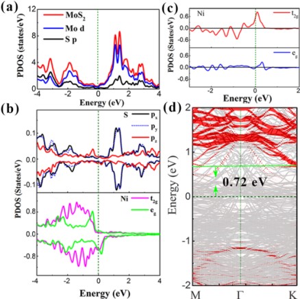
2 and (b) Ni and S atoms that form Ni-S bonds at the interface of the Ni (111)/MoS2 monolayer. (c) The differential DOSs (only the contribution from minority spin is shown) between Ni atoms at the interface and central region. (d) The band structure (grey solid lines) for Ni (111) on the MoS2 monolayer, in which only the minority bands are shown.” width=”438″ height=”436″ /> Figure 2: The PDOSs of (a) MoS2 and (b) Ni and S atoms that form Ni-S bonds at the interface of the Ni (111)/MoS2 monolayer. (c) The differential DOSs (only the contribution from minority spin is shown) between Ni atoms at the interface and central region. (d) The band structure (grey solid lines) for Ni (111) on the MoS2 monolayer, in which only the minority bands are shown.

Our calculations further show that when an additional MoS2 layer is introduced as a buffer layer as shown in Fig. 3(a), the strong interaction between Ni and the MoS2 channel layer can be decoupled. Thus, the strong interaction is confined at the interface between Ni and the MoS2 buffer layer, and does not extend into the MoS2 channel layer, as supported by the averaged charge density in Fig. 3(b). The MoS2 channel layer retains its semiconducting character, as well as a much reduced Schottky contact barriers (see Fig. 3(d)).
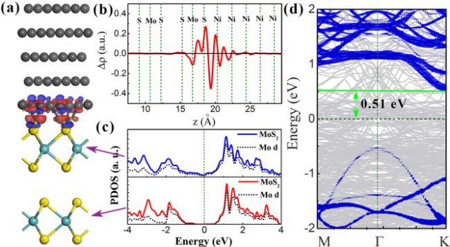
2 bilayer, in which the charge density difference is superimposed. (b) In-plane averaged charge density difference. (c) The PDOSs of the MoS2 bilayer. The blue and red solid lines denote the PDOS projected on the MoS2 buffer layer and lower MoS2 layer, respectively. (d) The band structure (grey solid lines) of Ni (111) on MoS2 bi-layers, in which only the minority bands are shown. The blue solid dots denote the contribution from Mo d orbitals in the lower MoS2 layer” width=”650″ height=”357″ /> Figure 3: (a) Side view of the most stable configuration for Ni (111) on the MoS2 bilayer, in which the charge density difference is superimposed. (b) In-plane averaged charge density difference. (c) The PDOSs of the MoS2 bilayer. The blue and red solid lines denote the PDOS projected on the MoS2 buffer layer and lower MoS2 layer, respectively. (d) The band structure (grey solid lines) of Ni (111) on MoS2 bi-layers, in which only the minority bands are shown. The blue solid dots denote the contribution from Mo d orbitals in the lower MoS2 layer

We wish to point out that the SBH can be further reduced to 0.29 eV by using the low work function metal Ti as the contact metal. Our results demonstrate the potential of using a MoS2 layer as an electrode buffer layer, and develop a simplified approach to improve contact performance between metals and 2D semiconductors. Due to the similar surface chemistry of 2D materials, our results might shed light on the understanding and integration of metal contacts with other 2D semiconductor materials.

Reference

Chai J. W., et al. Tuning Contact Barrier Height between Metals and MoS2 Monolayer through Interface Engineering, Adv. Mater. Interfaces 2017, 1700035.

NUS Information Technology | NUS IT Services, Solutions & Governance > Services > HPC Newsletter > » Interfacial Interaction between Metals and Monolayer MoS2 Revealed by First-Principles Calculations
ALCA
National University of Singapore
  • 2 Engineering Drive 4
  • NUS Information Technology
  • Singapore 117584
  • 6516 2080
  • © National University of Singapore. All Rights Reserved.
       Legal        Branding guidelines